All Products
-
Integrated Circuits (ICs)
- Integrated Circuits (ICs)
- AC to DC Converter ICs
- Active Filters
- ADC
- AFE
- Analog Multipliers & Dividers
- Analog Switches & Multiplexers ICs
- Application Specific Microcontrollers
- Application Specific Timer
- Audio Amplifiers
- Audio Special Purpose
- Battery Chargers ICs
- Battery Management ICs
- Buffers & Transceivers
- Capacitive Sensors
- Clock Buffers & Drivers
- Clock Generators
- CODECs Interface ICs
- Comparators
- Configuration Proms for FPGAs
- Controllers Interface ICs
- Converting Interface ICs
- Counters & Dividers
- CPLDs
- Current Regulator IC
- DAC
- DC DC Voltage Regulators
- DC to DC converter
- DDS
- Delay Lines Timing ICs
- Digital Potentiometers
- Display Drivers ICs
- Drivers Interface ICs
- DSP
- Embedded ICs Modules
- Energy Metering ICs
- FIFOs Memory
- Flip Flops
- FPGAs
- FPGAs with Microcontrollers
- Full & Half-Bridge Drivers ICs
- Gate Drivers ICs
- Gates & Inverters
- Hot Swap Controllers
- I/O Expanders
- IC Batteries
- Ideal Diode controller
- Instrumentational OP Amps
- Interface ICs Modules
- Laser Driver ICs
- Latches
- LED Driver ICs
- Lighting Controllers
- Linear Comparators
- Linear Regulator Controllers
- Linear Voltage Regulators
- Memory
- Memory Batteries
- Memory Controllers
- Microcontrollers
- Microprocessors
- Modems ICs & Modules
- Motor Drivers
- Multi-Functional Gates & Inverters
- Multivibrators
- Multivibrators
- PFC PMICs
- PLDs
- PoE Controllers
- Power Supply Control ICs
- Power Switches ICs
- Programmable Timers & Oscillators
- RMS to DC Converters
- RTCs
- Sensor & Detector Interface ICs
- Serializers & Deserializers
- Shift Registers
- Signal Buffers
- Signal Switches & Multiplexers
- Signal Terminators
- SoC
- Special Purpose ADCs/DACs
- Special Purpose Amplifiers
- Special Purpose Analog Switches
- Specialized ICs
- Specialized Interface ICs
- Specialized Power Management ICs
- Specialized Voltage Regulators
- Specialty Logic ICs
- Switching Voltage Regulators
- Telecom Interface ICs
- Thermal Management
- Touch Screen Controllers
- UARTs
- Universal Bus Functions
- V/F & F/V Converters
- Video Amps & Modules
- Video Processing Linear ICs
- Voice Record and Playback
- Voltage Reference
- Voltage Supervisors
- Voltage Translators & Level Shifters
-
Connectors
- Connectors
- ARINC Connectors
- Backplane Connector Contacts
- Backplane Connectors Accessories
- Backplane Connectors Housings
- Backshells and Cable Clamps
- Banana Tip Adapters
- Banana Tip Binding Posts
- Banana Tip Connectors Accessories
- Banana Tip Jacks
- Barrel Accessories
- Barrel Adapters
- Barrel Audio Connectors
- Barrel Connectors
- Barrel Power Connectors
- Barrier Terminal Blocks
- Between Series Adapters
- Blade Type Power Connectors
- Blade Type Power Connectors
- Blade Type Power Connectors Accessories
- Blade Type Power Connectors Housings
- Board In Connectors
- Board to Board Connectors
- Card Edge Adapters
- Card Edge Connectors Accessories
- Card Edge Connectors Housings
- Card Edge Contacts
- Centronics Connectors
- Circular Adapters
- Circular Connectors
- Circular Connectors Accessories
- Circular Connectors Housings
- Circular Contacts
- Coaxial Connectors
- Coaxial Connectors Accessories
- D-Sub Adapters
- D-Sub Connector Housings
- D-Sub Connector Terminators
- D-Sub Connectors
- D-Sub Connectors Accessories
- D-Sub Contacts
- D-Sub Hoods
- D-Sub Jackscrews
- DIN 41612 Connectors
- Din Rail Terminal Blocks
- Edgeboard Connectors
- Faceplates & Frames
- Fiber Optic Adapters
- Fiber Optic Connectors
- Fiber Optic Connectors Accessories
- Fiber Optic Connectors Housings
- Flat Flexible Connector Housings
- Flat Flexible Connectors
- Flat Flexible Connectors Accessories
- Flat Flexible Contacts
- Foil Connectors
- Hard Metric Connector
- Headers & Male Pins
- Heavy Duty Connectors Accessories
- Heavy Duty Connectors Assemblies
- Heavy Duty Connectors Frames
- Heavy Duty Connectors Housings
- Heavy Duty Connectors Modules
- Heavy Duty Contacts
- IC Adapters
- IC and Component Sockets
- IC Sockets Accessories
- Inline Memory Module Sockets
- Interface Modules Terminal Blocks
- Keystone Accessories
- Keystone Inserts
- Knife Connectors
- Leadframe Contacts
- LGH Connectors
- Magnetic Wire Terminals
- Magnetics Modular Jacks
- Memory Card Adapters
- Memory Card Sockets
- Memory Connectors Accessories
- Modular Adapters
- Modular Connectors Accessories
- Modular Jacks
- Modular Plug Housings
- Modular Plugs
- Multi Purpose Contacts
- Panel Mount Connectors
- Panel Mount Terminal Blocks
- PC Pin Terminals
- Photovoltaic Connectors
- Photovoltaic Connectors Accessories
- Photovoltaic Contacts
- Pluggable Connectors
- Pluggable Connectors Accessories
- Pluggable Terminal Blocks
- Power Distribution Terminal Blocks
- Power Entry Connectors Accessories
- Power Entry Connectors Modules
- Quick-Connect & Quick-Disconnect Connectors
- Rectangular Connectors
- Rectangular Connectors Accessories
- Rectangular Connectors Adapters
- Rectangular Connectors Arrays
- Rectangular Connectors Headers
- Rectangular Connectors Housings
- Rectangular Contact Inserts
- Rectangular Terminals
- RF Adapters
- RF Contacts
- RF Terminators
- Ring Terminals
- Screw Connectors
- Shunts & Jumpers
- Socket Terminals
- Solder Lug Connectors
- Spade Connectors
- Specialized Backplane Connectors
- Specialized Connectors
- Specialized Terminal Blocks
- Spring Loaded Contacts
- Spring Loaded Rectangular Connectors
- SSL Connectors
- SSL Connectors Accessories
- SSL Contacts
- Terminal Block Adapters
- Terminal Blocks - Contacts
- Terminal Blocks Accessories
- Terminal Jumpers
- Terminal Junction Systems
- Terminal Marker Strips
- Terminal Strips and Turret Boards
- Terminal Wire Ferrules
- Terminals Accessories
- Terminals Adapters
- Terminals Housings
- Transistor Sockets
- Turret Connectors
- Video Adapters
- Video Connector Accessories
- Video Connectors
- Wire Pin Connectors
- Wire Splice Connectors
- Wire-to-Board Connectors
- Wire-to-Board Terminal Blocks
- Wiring Blocks Accessories
- Wiring Modular Connectors
-
Discrete Semiconductors
- Discrete Semiconductors
- Arrays BJT Transistors
- BJT Transistors Arrays
- Bridge Rectifiers
- DIACs and SIDACs
- IGBTs Modules
- IGBTs Transistors Arrays
- JFETs Transistors
- MOSFETs Transistors Arrays
- Power Driver Modules
- Pre-Biased BJT Transistors
- Programmable Unijunction Transistors
- Rectifier Diode Array
- RF BJT Transistors
- RF Diodes
- RF MOSFETs Transistors
- SCRs Thyristors
- Single BJT Transistors
- Single IGBTs
- Single IGBTs
- Single MOSFETs Transistors
- Single-Phase Diode Rectifier
- Specialized Transistors
- Thyristors Modules
- TRIACs Thyristors
- Varactors
- Zener Diode Arrays
- Zener Single Diodes
-
Capacitors
- Capacitors
- Aluminum Electrolytic Capacitors
- Aluminum Polymer Capacitors
- Capacitor Accessories
- Capacitor Networks
- Ceramic Capacitors
- Ceramic Capacitors
- Film Capacitors
- Mica & PTFE Capacitors
- Niobium Oxide Capacitors
- Silicon Capacitors
- Supercapacitors & EDLC
- Tantalum Capacitors
- Tantalum Polymer Capacitors
- Thin Film Capacitors
- Trimmers Variable
-
Sensors
- Sensors
- CdS Cells
- Accelerometers
- Accessories
- Amplifiers
- Analog & Digital Sensor
- Analog & Digital Sensors
- Analog Optical Sensors
- Angle & Linear Position Measuring Sensors
- Camera Modules
- Color Sensors
- Current Sensors
- Distance Measuring Sensors
- Dust Sensors
- Encoders
- Float & Level Sensors
- Flow Sensors
- Force Sensors
- Gas Sensors
- Gyroscopes
- Humidity Sensors
- Image Sensors
- IMUs
- Inclinometers
- IrDA Transceiver Modules
- Junction Blocks
- Logic Optical Sensors
- Logic Photo Detectors
- Logic Photointerrupters
- LVDT Transducers
- Magnetic Compass Sensors Modules
- Magnetic Linear Sensors ICs
- Magnetic Position Sensors Modules
- Magnetic Switches
- Mechanical Temperature Sensors
- Multi Purpose Magnets
- Multifunction
- NTC Thermistors
- Occupancy Sensors
- Optical Motion Sensors
- Optical Sensors Remote Receiver
- Photodiodes
- Photoelectric Sensors
- Phototransistors
- Proximity Sensors
- PTC Thermistors
- RTD
- Sensor Cable Accessories
- Sensor Cable Assemblies
- Sensor Matched Magnets
- Shock Sensors
- Solar Cells
- Solid State Thermostats
- Specialized Sensors
- Strain Gauges
- Thermocouple Temperature Sensors
- Tilt Switch Sensors
- Touch Sensors
- Transducers
- Transistor Optical Sensors
- Ultrasonic Receivers
- UV Sensors
- Vibration Sensors
- Resistors
- Isolators
- Board Mount Poser Supplies
-
RF/IF & RFID
- RF/IF & RFID
- Attenuators
- Balun
- RF Accessories
- RF Amplifiers
- RF Antennas
- RF Boards
- RF Demodulators
- RF Detectors
- RF Directional Coupler
- RF Front End
- RF Misc ICs and Modules
- RF Mixers
- RF Modulators
- RF Multiplexers
- RF Power Controller ICs
- RF Power Dividers
- RF Receivers
- RF Shields
- RF Switches
- RF Transceiver ICs
- RF Transceiver Modules
- RF Transmitter
- RF Transmitters
- RFI & EMI Contacts
- RFI & EMI Materials
- RFID Accessories
- RFID Antennas
- RFID Boards
- RFID ICs
- RFID Reader Modules
- RFID Tags
- Circuit Protection
- Crystals
- Inductors
- Filters

DS25BR100TSD/NOPB
You may place an order without registering to XINJIADA.
We strongly suggest you sign in before purchasing as you
can track your order in real time.
For your convenience, we accept multiple payment methods in USD, including PayPal, Credit Card, and wire transfer.
RFQ (Request for Quotations)It is recommended to request for quotations to get the latest
prices and inventories about the part.
Our sales will reply to
your request by email within 24 hours.
1. You'll receive an order information email in your inbox.
(Please remember to check the spam folder if you didn't hear from us).
2. Since inventories and prices may fluctuate to some
extent, the sales manager is going to reconfirm the order and let you know if there
are any updates.
Shipping starts at $40, but some countries will exceed $40. For
example (South Africa, Brazil, India, Pakistan, Israel, etc.)
The
basic freight (for package ≤0.5kg or corresponding volume) depends on the time zone and
country.
Currently, our products are shipped through DHL, FedEx, SF, and UPS.
Delivery TimeOnce the goods are shipped, estimated delivery time depends on the shipping methods you chose:
FedEx International, 5-7 business days.
The following are some common countries' logistic time.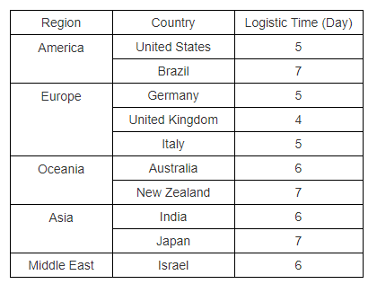
| Parameters | |
|---|---|
| Factory Lead Time | 16 Weeks |
| Lifecycle Status | ACTIVE (Last Updated: 1 day ago) |
| Contact Plating | Tin |
| Mount | Surface Mount |
| Mounting Type | Surface Mount |
| Package / Case | 8-WFDFN Exposed Pad |
| Number of Pins | 8 |
| Operating Temperature | -40°C~85°C |
| Packaging | Tape & Reel (TR) |
| JESD-609 Code | e3 |
| Pbfree Code | yes |
| Part Status | Active |
| Moisture Sensitivity Level (MSL) | 3 (168 Hours) |
| Number of Terminations | 8 |
| Type | Buffer, ReDriver |
| Applications | LVDS |
| Subcategory | Line Driver or Receivers |
| Max Power Dissipation | 2.08W |
| Voltage - Supply | 3V~3.6V |
| Terminal Position | DUAL |
| Peak Reflow Temperature (Cel) | 260 |
| Number of Functions | 1 |
| Supply Voltage | 3.3V |
| Terminal Pitch | 0.5mm |
| Base Part Number | DS25BR100 |
| Pin Count | 8 |
| Operating Supply Voltage | 3.3V |
| Number of Elements | 1 |
| Operating Supply Current | 35mA |
| Nominal Supply Current | 43mA |
| Power Dissipation | 2.08W |
| Propagation Delay | 465 ps |
| Turn On Delay Time | 465 ps |
| Max Output Voltage | 450mV |
| Min Input Voltage | -100mV |
| Max Input Voltage | 100mV |
| Output Characteristics | DIFFERENTIAL |
| Differential Output | YES |
| Input | CML, LVDS, LVPECL |
| Output Polarity | COMPLEMENTARY |
| Power Consumption | 115W |
| Driver Number of Bits | 1 |
| Max Input Current | 10μA |
| Interface Standard | GENERAL PURPOSE |
| Data Rate (Max) | 3.125Gbps |
| Transmit Delay-Max | 0.465 ns |
| Supply Voltage1-Nom | 3.3V |
| Delay Time | 350ps |
| Capacitance - Input | 1.7pF |
| Signal Conditioning | Input Equalization, Output Pre-Emphasis |
| Height | 800μm |
| Length | 3mm |
| Width | 3mm |
| Thickness | 800μm |
| Radiation Hardening | No |
| RoHS Status | ROHS3 Compliant |
| Lead Free | Lead Free |
DS25BR100TSD/NOPB Overview
Packaging is convenient because power buffer comes in 8-WFDFN Exposed Pad.Package number Tape & Reel (TR) is ready for power buffer.It comes with a universal mout that allows for easy adaptation.Speaking of types, this is a typical Buffer, ReDriver.The op amp buffer uses a voltage of 3V~3.6V volts for its operation.The system facilitates the input of CML, LVDS, LVPECL.A -40°C~85°C should be set as the operating temperature in order to avoid malfunctions.The operational amplifier buffer is targeted at applications such as LVDS and others.It is possible to search with "DS25BR100" to get more pin-to-pin solutions for your special requirements if you are looking for some.It is possible to find 8 terminals on the op amp buffer of the assembly.Its peak reflow temperature is 260.3.3V voltage enables the splitter to handle a wide range of demanding tasks.Taking the Power buffer's pinout as an example, it starts from the 8 pins it has on its surface.8 pins are present on the op amp buffers.The Surface Mount on the board allows it to be mounted on PCBs or other boards.There are other Line Driver or Receivers's in the industry that play a significant role, like the power buffer.The power buffer is powered by 35mA voltage.For normal operation, 3.3V voltage is required.The splitter dissipates at most 2.08W watts.Normally, 43mA is the supply current for this splitter.The repeater signal is a 1 element interface.
DS25BR100TSD/NOPB Features
Mainly used in LVDS.
A standard Line Driver or Receivers.
DS25BR100TSD/NOPB Applications
There are a lot of Texas Instruments DS25BR100TSD/NOPB Signal Buffers, Repeaters, Splitters applications.
- Clock Distribution
- DSLAMs
- PECL-to-LVDS Translation
- Protection Switching
- Add/Drop Muxes
- Clock Distribution
- Network Switches/Routers
- Digital Crossconnects
- SATA SSDs or HDDs
- Communications Switchers
 10,000+
Daily Order Quantity
 5000,000+
Alternative Parts
 2800+
2800+Worldwide Manufacturers
 15,000 ㎡
In-stock Warehouse


